
 Existing User
Already have a account?
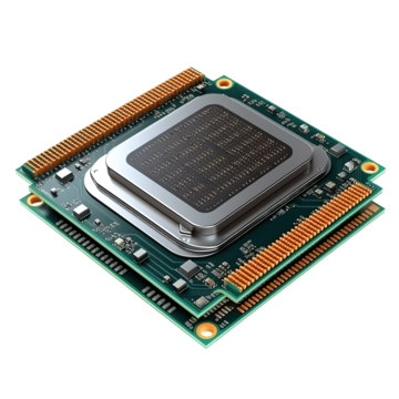
Design Linked incentive (DLI)
The Design Linked Incentive (DLI) Scheme aims to offer financial incentives as well as design infrastructure support across various stages of development and deployment of semiconductor design(s) for Integrated Circuits (ICs), Chipsets, System on Chips (SoCs), Systems & IP Cores and semiconductor linked design(s) over a period of 5 years.
Procedure to Apply
Registration
Submission of relevant information to register with DLI and submit application
Proposal
Detailed Project Report
Payment of Fee
Application fee as per Scheme and Guidelines.
Fiscal Support
Fiscal Support to domestic companies, Startups and MSMEs
Automation (EDA) Tool Grid
Contact Us
Mr. Nishit Gupta
Scientist 'E', MeitY
: Electronics Niketan, CGO Complex Lodhi Road, New Delhi -
110003
: support[DOT]chips[HYPHEN]dli[AT]cdac[DOT]in
: +91-9560924355
: +91-11-24301249
Mr. Abhishek Tiwari
Joint Director,
C-DAC, Noida
: C-56/1, Sector-62, Noida - 201307, Uttar Pradesh (India)
:
support[DOT]chips[HYPHEN]dli[AT]cdac[DOT]in, pmudli[AT]cdac[DOT]in
:
+91-8920175458
:
+91-120-2210890