


-
DLI Portal & PMU
C-56/1, Sector-62, Noida - 201307, Uttar Pradesh (India)support[DOT]chips[HYPHEN]dli[AT]cdac[DOT]inpmudli[AT]cdac[DOT]in+91-120-2210800 (Ext 721)Mr. Nishit Gupta Scientist-E, MeitY
Electronics Niketan, CGO Complex Lodhi Road, New Delhi - 110003support[DOT]chips[HYPHEN]dli[AT]cdac[DOT]in+91-9560924355+91-11-24301249Mr. Abhishek Tiwari Scientist-F, C-DAC, Noida
C-56/1, Sector-62, Noida - 201307, Uttar Pradesh (India)support[DOT]chips[HYPHEN]dli[AT]cdac[DOT]in+91-8920175458+91-120-2210890
 Important News

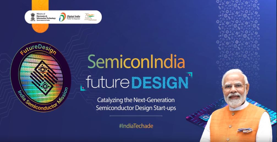
The Design Linked Incentive (DLI) Scheme
About us
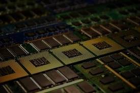
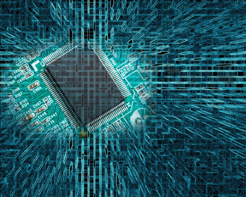
Semiconductors are at the heart of all electronic products and constitute a significant share in the Bill of Material (BOM). The National Policy on Electronics 2019 aims to position India as a global hub for Electronics System Design and Manufacturing (ESDM) and envisions creation of a vibrant semiconductor chip design ecosystem in the country. With an exceptional talent pool of 20% of world's semiconductor design engineers and thousands of chips designed by them every year in the country, India is poised for growth to achieve self-reliance and technology leadership in semiconductor design sector. Ministry of Electronics and Information technology has announced the Design Linked Incentive (DLI) Scheme to offset the disabilities in the domestic industry involved in semiconductor design in order to not only move up in value-chain but also strengthen the semiconductor chip design ecosystem in the country. CDAC is responsible for implementation of the DLI Scheme as Nodal Agency. The Design Linked Incentive (DLI) Scheme aims to offer financial incentives as well as design infrastructure support across various stages of development and deployment of semiconductor design(s) for Integrated Circuits (ICs), Chipsets, System on Chips (SoCs), Systems & IP Cores and semiconductor linked design(s) over a period of 5 years.
Objectives
- Nurturing and facilitating the growth of the domestic companies, startups and MSMEs.
- Achieving significant indigenization in semiconductor content and IPs involved in the electronic products deployed in the country, thereby facilitating import substitution and value addition in electronics sector.
- Strengthening and facilitating access to semiconductor design infrastructure for the startups and MSMEs.
Eligibility
Financial incentives and design infrastructure support will be extended to domestic companies, Startups and MSMEs engaged in semiconductor design or semiconductor linked design. The approved applicants that claim incentives under the scheme shall retain their domestic status (i.e. more than 50% of the capital in it is beneficially owned by resident Indian citizens and/ or Indian companies, which are ultimately owned and controlled by resident Indian citizens) for a period of three years after claiming incentives under the scheme. An applicant must meet the Threshold and Ceiling Limit to be eligible for disbursement of incentive as indicated here (Threshold and Ceiling Limits).
Scheme Tenure
In accordance with Para 4 of the Scheme, the Application Window shall be initially three (3) years from 01-01-2022.
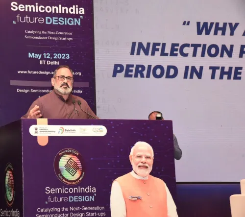
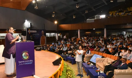
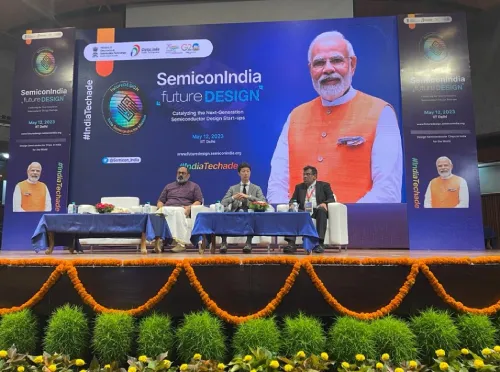
Events & Activities

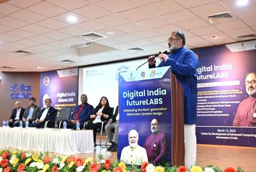
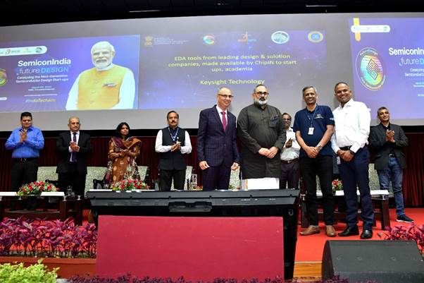
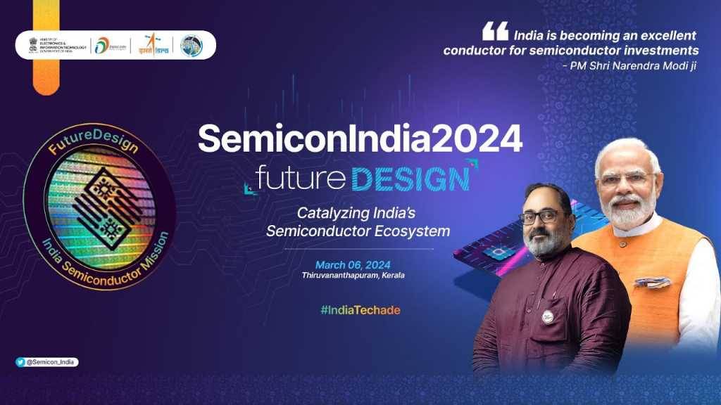
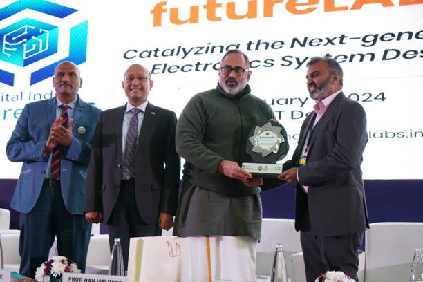
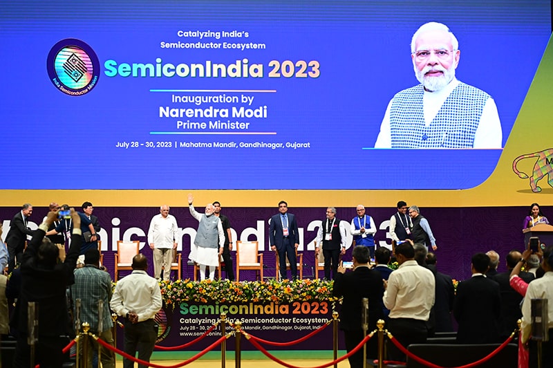
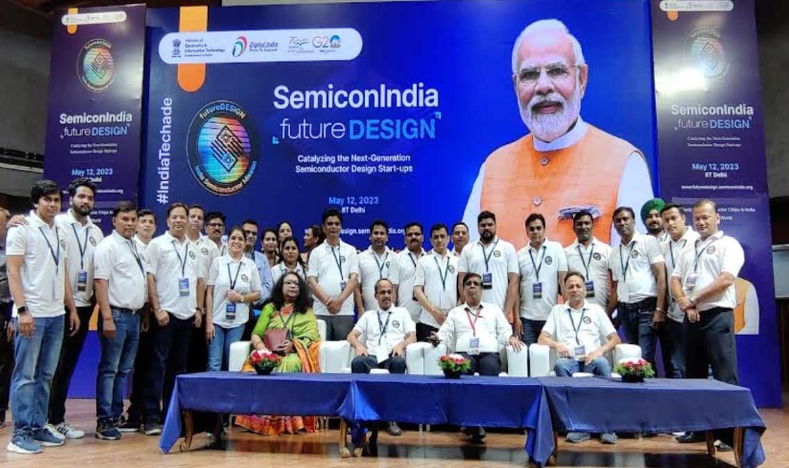
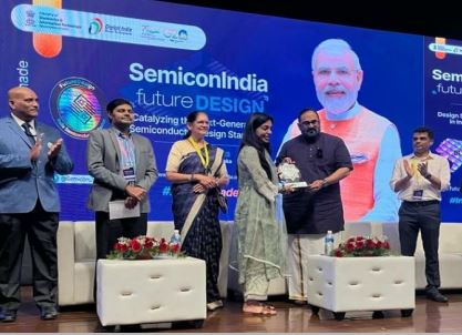
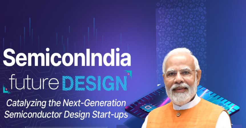
Latest Announcements
- Announcements Icon Union Minister Shri Ashwini Vaishnaw interacts with Semiconductor Chip Design Companies approved under the DLI Scheme
- Announcements Icon Design Linked Incentive Scheme Catalyzing India’s Semiconductor Design Ecosystem.
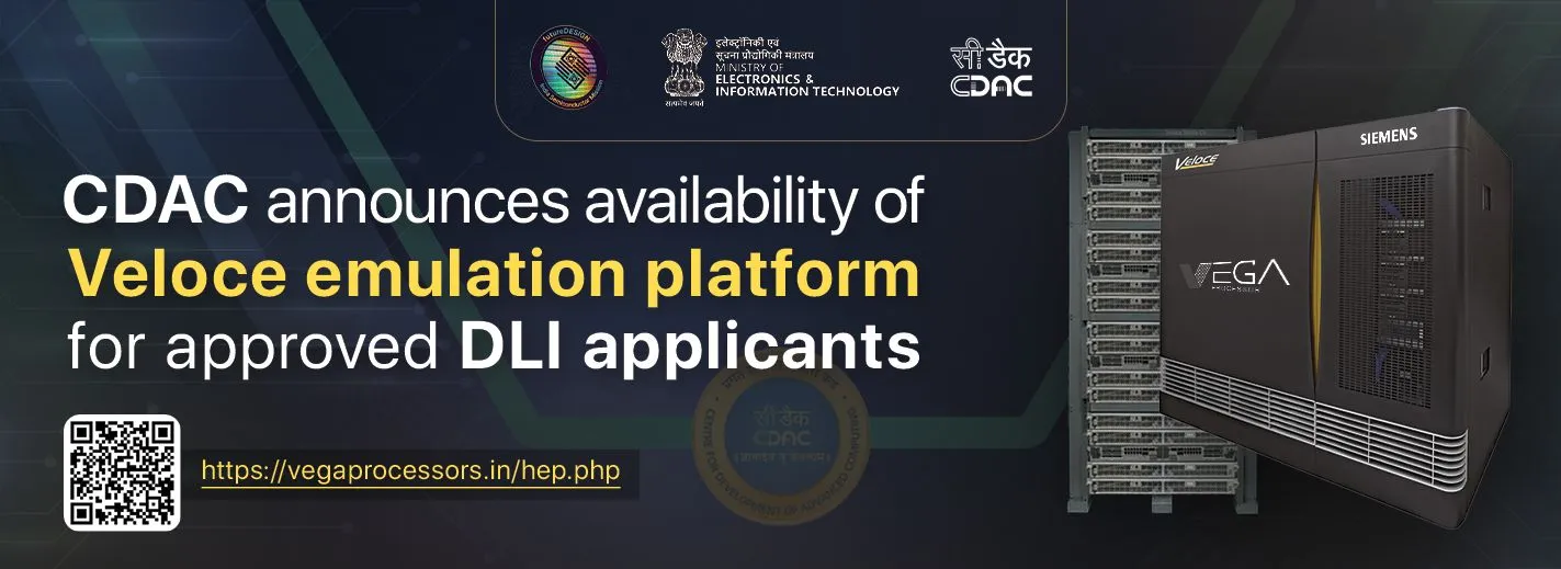
- Announcements Icon Availability of CDAC Veloce Hardware Emulator platform to approved DLI applicants
- Announcements Icon Support under Arm Flexible Startup Program free of cost to DLI applicants
- Announcements Icon List of companies supported under PDLI
- Announcements Icon List of Companies supported for EDA tools
- Announcements Icon Nanofabrication and Characterization Facilities
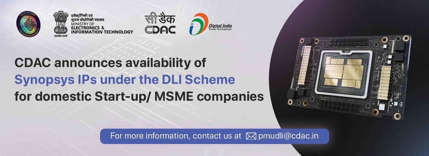
- Announcements Icon Availability of Synopsys IPs
Beneficiaries
DLI Beneficiaries
The Design Linked Incentive (DLI) scheme supports startups and companies in semiconductor design and innovation. These beneficiaries are building solutions that strengthen India’s electronics ecosystem.
Programme Highlights
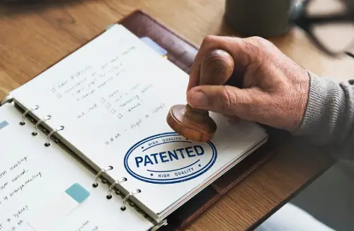
Patents
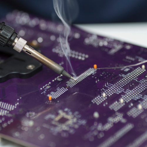
Designs Taped Out
ASICs
Fabricated

Specialized
Manpower
IP
Generated
Hours of EDA
tools used
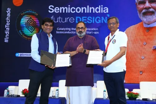
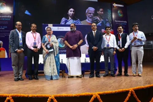
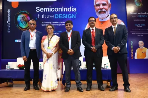
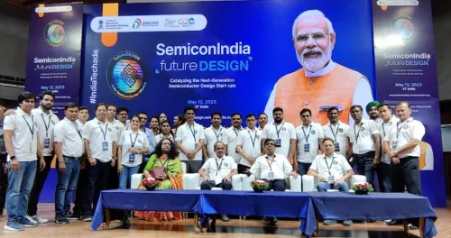
Gallery
Visual Highlights
Testimonials
Endorsements from Leadership
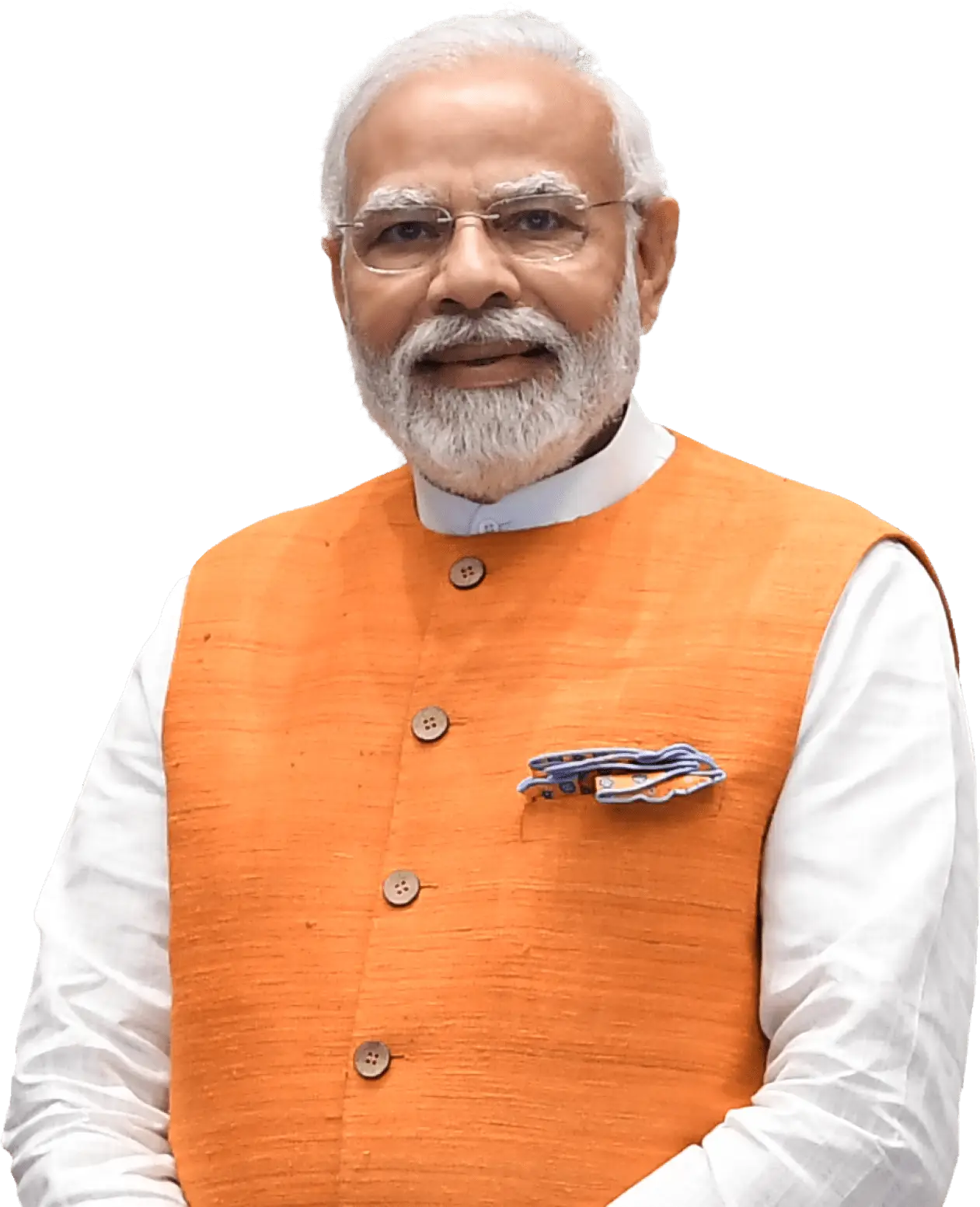
Testimonial Quote Left Icon It is our collective aim to
establish India as one of the key partners in global
semiconductor supply chains. Testimonial Quote Right Icon
Shri Narendra
Modi
Hon'ble Prime Minister of India

Testimonial Quote Left Icon India emerging as the most
important ecosystem partner in semiconductors.Testimonial Quote Right Icon
Shri Ashwini
Vaishnaw
Hon'ble Minister of Railways,
Information and Broadcasting and
Electronics & Information Technology,
Government Of India
Information and Broadcasting and
Electronics & Information Technology,
Government Of India
Applications
Overview of all application statuses
Received
PDLI
PDLI State NumberEDA
EDA State Number
Approved
PDLI
PDLI State NumberEDA
EDA State Number
In Review
PDLI
PDLI State NumberEDA
EDA State Number
Not Accepted in Present Form
PDLI
PDLI State NumberEDA
EDA State Number
Claim
Received
Received State NumberSettled
Settled State Number
Accessibility Options
Adjust Font Size
100%
Highlight Links
Highlight Titles
Text Spacing
Line Height
Text Alignment
Dyslexia Font
Color Adjustments
Light Theme
Invert Colors
Other Accessibility Features
Pause Animations
Hide Images
Custom Cursor
Text to Speech
ADHD Mode